Major projects aligned with the goals of the EU Chips Act are starting to emerge, positioning research organisations to take advantage of new funding

With legislative work on the EU Chips Act making slow but steady progress, research organisations are starting to come forward with projects that meet its goal of developing the European ecosystem for semiconductor start-ups and scale-ups. The latest to unveil plans are the Research Fab Microelectronics Germany and a group led by VTT Technical Research Centre of Finland and Aalto University.
The two projects will look beyond conventional complementary metal-oxide semiconductor (CMOS) technology to more specialised applications, in particular related to quantum computing. “There is a strong link between the quantum technology and the different components that are needed for quantum, and then the other semiconductor applications,” said Erka Turunen, executive vice president for digital technologies at VTT.
Highlighting innovation is also a way that smaller countries such as Finland can find a role in the Chips Act, which is mostly focused on building major fabrication facilities to increase Europe’s strategic autonomy in semiconductors. “I don’t think it is realistic to think that there will be a CMOS factory in Finland, but this could be the way that Finland could participate in the Chips Act,” Turunen said.
Start-ups and scale-ups will get some direct support under the EU Chips Act, through a combination of new and repurposed funding. The European Innovation Council has €300 million to spend on Chips Act priorities, for example through its Accelerator programme, while the European Investment Bank has funds to channel to companies and venture capital funds for co-investment in small European semiconductor companies.
Layered above support for individual companies are initiatives intended to help the whole start-up ecosystem. There will be a cloud-based virtual design platform, bringing together a wide range of design libraries, tools and support services, which should lower the costs for start-ups hoping to enter the semiconductor market. A network of competence centres will be set up across Europe, to address the shortage of trained staff and students interested in entering the field.
But in order to meet the innovation goals of the EU Chips Act, there is a need for new, specialist infrastructure, and this is where national research organisations are starting to position themselves.
The aim of the German project announced this month is to add a quantum and neuromorphic computing (QNC) module to the Research Fab Microelectronics Germany (FMD), a collaboration between 11 Fraunhofer institutes and two Leibniz institutes working on R&D and pilot production of semiconductor-based micro- and nanosystems. The FMD-QNC module will support researchers and companies developing microelectronics and scalable manufacturing and integration processes for these new computing technologies.
In addition to the current FMD partners, the module will draw in four other Fraunhofer institutes, together with the Jülich Forschungszentrum and the nanotech company AMO. Over the next three years, the partners will be equipped with design tools, measurement and characterisation techniques, and the manufacturing facilities required for application-oriented research into quantum and neuromorphic computing.
The plan is to offer partners from both science and industry flexible, low-threshold access to the facilities for preliminary research, technology development and pilot production. There will be a space for testing special manufacturing methods, and an open design platform. The German Federal Ministry of Education and Research will fund both the equipment and structural setup required for the project.
Meanwhile, the Fraunhofer institutes are working with European partners to address other priorities under the Chips Act. For example, the Partnership for Realisation and Validation of AI hardware Leadership (Prevail) brings together CEA-Leti, Fraunhofer, imec and VTT to establish a networked 300mm technology platform for the fabrication of chip prototypes used in advanced artificial intelligence and neuromorphic computing applications.
Germany’s contribution will come from four Fraunhofer institutes belonging to the FMD, which will broaden their 300mm fabrication, design and test facilities. “The intended project activities within Prevail and FMD-QNC will be synergistically interconnected and represent an essential preparatory work for the technological foundation of the European Chips Act,” the FMD said in a statement.
Piloting environment
The Finnish plan is to build a piloting environment that will offer companies in the growth phase a resource to scale up their innovations. “You need to be a pretty big company, with good funding, before you can start to establish manufacturing capabilities by yourself,” said Turunen. “That is the gap we want to fill, giving cheaper and easier access for growth companies to do their own R&D and start to scale-up for production.”
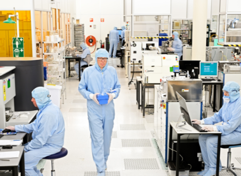
The project has been put together by VTT, the city of Espoo, Aalto University and companies in the Technology Industries of Finland semiconductor group. The idea is to expand existing research infrastructure for microelectronics and quantum computing located in Espoo, notably the Micronova centre run jointly by VTT and Aalto University, which offers cleanrooms and equipment to companies carrying out R&D.
Currently around 20 companies make use of the facility. The new project will extend that with further clean rooms and facilities for piloting, to be built nearby. “It would be a combined environment, with jointly used equipment and also the possibility for companies to have their own spaces, for their own equipment and production,” Turunen said.
The goal is to foster a spirit of open innovation. “It’s not only the facilities, but also the way we can co-develop projects, so that companies and researchers can learn from each other and innovate together. So, it’s the whole ecosystem, the whole hub, that is important, not just the building and the equipment,” said Turunen.
Turunen is keen to point out that the companies are the driving force behind the initiative. “They see it as important for their innovation, their development and their growth, that we have this kind of facility.”
The Technology Industries of Finland semiconductor group includes both Huawei and Chinese-owned Okmetic, which might raise eyebrows when it comes to an initiative aiming to contribute to Europe’s strategic autonomy in semiconductors.
Turunen acknowledges that the question deserves discussion, at the European level. “We need to think about how the relationship between the different continents will develop in future, how we protect core intellectual property (IP), and then who are then the correct partners for us to develop core IP with.”
The involvement of foreign interests should not pose a problem for the pilot environment project, where all actions will be set out in specific, project-based agreements. But more thought on the broader issues is required. “We need a common European approach to how we are dealing with these matters,” Turunen said.
The total budget for the pilot environment is estimated at €90 million. According to current estimates, approximately half would be public funding, for example in the form of funding applied through the European Chips Act. Being able draw on this resource depends on the funds given to its first pillar, which covers technological capacity building and innovation in the EU chips ecosystem.
“We feel that it’s important for Europe to invest across all the pillars. Of course, we need to ensure the mass production capabilities for the CMOS and so forth, but Europe also needs joint investment for the first pillar activities. Other kinds of semiconductor innovations and technologies, such as silicon photonics, will be very important in the future, and we also have to invest in those,” said Turunen.
She also thinks that spreading investments will be important if the Chips Act is to be a strategy for the whole of Europe. “It is very important that we develop European networks and complementary investments in different parts of Europe so that the whole European infrastructure is serving European companies in the best way and avoid creating silos in Europe.”
The current plan is to begin building work on the pilot environment in 2024, assuming the funding can be secured. And if the Chips Act does not provide enough to develop the project, other sources will be required. In that case, the project has a lot to recommend it. “This is a way to attract new investments to Finland, and VTT has a lot of international customers who are looking for good R&D hubs to invest in, so we see that the payback will be there.”
Elsewhere in the Ecosystem…
- Spanish start-up DeepUll has been granted a €20 million loan from the European Investment Bank (EIB) for the development of an automated device that promises faster and more accurate early diagnosis of sepsis. This follows the closure in October of a €13 million series B funding round. DeepUll was founded in Barcelona in 2020 by the founders of STAT-Dx, which was sold to Qiagen in 2018. The loan is financed through the EIB’s Infectious Diseases Finance Facility, set up as part of Horizon 2020.
- Early-stage venture capital fund Speedinvest has raised €500 million in new capital, of which €300 million will go into pre-seed and seed funding for European tech start-ups. The rest is reserved for follow-on co-investments in companies already in the portfolio. Investors contributing to the round include founders from several start-ups previously supported by Speedinvest, such as battery analytics company Twaice, climate tracker Planetly, education platform GoStudent, and fintechs Bitpanda, Billie and Yokoy. The new capital will give Speedinvest more than €1 billion assets under management.
- The European Institute of Innovation and Technology’s Urban Mobility community has announced a collaboration with Israeli acceleration programme 8200 Impact and Tel Aviv living lab CityZone. The aim is to build bridges between the European and the Israeli mobility ecosystems and support start-ups from both sides. Among other activities, 8200 Impact and CityZone will host a two-month acceleration programme for European and Israeli start-ups focusing on inclusive mobility. Meanwhile, EIT Urban Mobility will invest up to €500,000 each in two early-stage Israeli start-ups, which will also benefit from piloting opportunities in European cities.


 A unique international forum for public research organisations and companies to connect their external engagement with strategic interests around their R&D system.